Intel’s new Atom chips peak on performance, power consumption
http://www.cnmeonline.com/news/intels-new-atom-chips-peak-on-performance-power-consumption/
by Agam Shah - May 7th, 2013
 Intel’s upcoming Atom chips with new CPU architecture will be up to three times faster and five times more power efficient than their predecessors and break the “myth” that ARM processors are more power efficient, Intel said.
Intel expects the new architecture, code-named Silvermont, to be in smartphones, tablets, PCs and servers starting this year. Atom chips code-named Bay Trail will appear in tablets this holiday season. They will support the Android and Microsoft operating systems.
Tablet chips based on Silvermont are two times faster on single-threaded performance than comparable chips based on the current Atom architecture code-named Saltwell, said Belli Kuttanna, an Intel fellow during a briefing Monday that was webcast. Using the same metric, Kuttanna said that Silvermont tablet chips use 4.7 times less power than their predecessors.
Bay Trail chips will also appear in hybrid laptops with detachable and folding screens, and in low-cost desktops priced from $200 to $599. Users can choose between long battery or performance in Silvermont smartphones or tablets, Kuttanna said.
“Silvermont is a complete redefinition of the Atom architecture,” Kuttanna said.
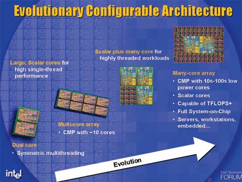
Silvermont CPUs can scale up to eight cores and represent the first major redesign of the Atom architecture since the first netbook chip release in 2008. Atom chips with Silvermont will also include new performance and power management features.
Silvermont comes at a time when the chip maker is trying to find its footing in the smartphone and tablet markets. Intel hopes that Bay Trail will attract a new set of PC buyers and give it a legitimate shot to compete against ARM, which rules the smartphone and tablet markets.
Previous Atom chips were panned for poor performance compared to ARM, whose reputation lies with maximising power efficiency on chips. Intel has maintained that it has already caught up with ARM on power efficiency with the recent Atom chips code-named Medfield, which are used in smartphones.
But during the webcast, Intel Chief Product Officer Dadi Perlmutter said that Atom chips based on Silvermont will offer better performance-per-watt and break the “myth” that ARM processors are more power efficient.
“We see that this kind of solution will be even better,” said Perlmutter, who is also the executive vice president and general manager of the Intel Architecture Group.
Silvermont CPUs incorporate a number of improvements. Out-of-order execution enables more efficient processing of instructions via clock cycles and chips will have more internal bandwidth, with a faster fabric that connects the CPU to other processors such as GPUs. In addition, Silvermont is able to move data faster from the shared cache into DRAM, which enables quicker task execution.
Silvermont also includes the latest virtualisation and security technologies, some of which has been borrowed from previous Intel chip architectures for servers and PCs.
The cores are also flexible on performance and power consumption. CPU cores can be clocked up or shut down if idle. Intel said the flexibility provided by its cores is a better option than ARM’s Big.Little, which incorporates different types of CPU cores to meet power and performance needs. Samsung’s Exynos 5 Octa eight-core processor incorporates a Big.Little design with four high-power cores for demanding tasks and four low-power cores for tasks MP3 playback and voice calls.
With Intel’s chip, no switching would be needed between low-power and high-power cores to meet different performance needs, Kuttanna said. A single Silvermont core can cover different ranges of power and performance, with no algorithms required to switch between cores.
“We can go up and down the range and cover the entire performance range,” Kuttanna said. “You don’t pay the complexity price.”
The new architecture is also able to share power between CPUs, graphics processors and other cores in a chip. Algorithms can also monitor power delivery, thermal and electrical features, and bring power consumption down based on the device type. Tablets and smartphones will also be able to resume from idle mode a lot quicker with new Silvermont features.
Atom chips based on Silvermont will be made using the 22-nanometre process, in which a 3D transistor allows more transistors in a smaller space. The chip will be smaller and more power efficient than the current Atom chips code-named Clover Trail, which are based on the 32-nm process.
Intel is advancing to the 14-nm process later this year, but the company hasn’t said when new smartphone and tablet chips based on the process will be released. Intel Atom’s chips made using 14-nm manufacturing technology are called “Airmont.”
英特爾發表低功耗高效能的 Silvermont 微架構 [2013/05/07 18:13]
http://iservice.libertytimes.com.tw/3c/news.php?no=9368&type=3
英特爾發表名為 Silvermont 的全新低功耗、高效能微架構。
這項技術主要是為了智慧型手機到資料中心等有低功耗需求的市場所設計。 Silvermont 將成為許多創新產品的基礎,而這些產品將於今年稍後問市,其晶片是採用英特爾的先進 22 奈米三閘( Tri-Gate )系統單晶片( SoC )製程,以帶來大幅增進的效能與電源使用效益。
英特爾產品長暨執行副總裁 Dadi Perlmutter 表示:「 Silvermont 不僅是一大進步,也將作為未來嶄新技術的基礎,能滿足各種產品與市場的需求。包括代號為『 Bay Trail 』與『 Avoton 』在內的 22 奈米系統單晶片的初步樣本已獲得客戶的正面好評。未來我們將加快發展此低功耗微架構,每年都會推出新一代技術。」
Silvermont 微架構帶來領先業界的每瓦效能。高度均衡化的設計可支援更廣的動態範圍,並無縫地調升與調降效能以及電源使用效益。在各種標準中, Silvermont 亦提供比目前 Intel Atom (凌動 )處理器核心 1 高達 3 倍的尖峰效能,或者在相同效能水準下,耗電量降低至五分之一。
Silvermont :新一代微架構
英特爾的 Silvermont 微架構運用英特爾的 22 奈米系統單晶片製程進行設計與協同最佳化,並採用革命性的 3-D 三閘電晶體。英特爾藉由這項領先業界的技術帶來大幅的效能提升並增進電源使用效益。
Silvermont 微架構的其他特性還包括:
- 全新亂序( out-of-order )執行引擎,帶來先進的單執行緒( single-threaded )運算效能。
- 新的多核心與系統互連架構,最多可擴充至八核心,進一步推升效能以支援高頻寬、低延遲、以及更有效率的亂序處理模式,打造出更均衡化且快速反應的系統。
- 新的 IA 指令集與技術,帶來進階的效能、虛擬化、以及安全管理功能,藉以支援各類型的產品。這些指令集建立在英特爾現有的 64 位元支援技術以及已安裝的 IA 軟體基礎。
- 增強的電源管理功能,包括新的智慧遽增技術( intelligent burst technology )、各種低功耗休眠狀態、以及運用英特爾 3-D 電晶體帶來更廣的動態運作範圍。 Intel Burst Technology 2.0 支援單核與多核心晶片,提供更快的反應速度進而增進電源使用效益。
英特爾院士暨首席架構工程師 Belli Kuttanna 表示:「藉由設計與製程技術的協同最佳化,超越我們原先對 Silvermont 設下的各項目標。我們善加運用在微架構研發與尖端製程技術的實力,推出一個最佳技術組合,讓業者大幅提升效能與電源使用效益,同時提供更高的時脈頻率。我們以這項成就為榮,並相信 Silvermont 將為眾多新款低功耗英特爾系統單晶片提供強大且富彈性的基礎。」
針對各領域的運算量身打造
Silvermont 將作為一系列 22 奈米產品的基礎,產品將在今年稍後陸續問市。此新微架構提升了每瓦效能,將使採用這些產品的運算裝置獲得大幅增進的效能與反應速度。
內含英特爾四核心系統單晶片(代號為 Bay Trail )的平板電腦將於 2013 年聖誕假期上市,其運算效能是目前內含英特爾處理器平板電腦 1 的兩倍以上。受益於 Silvermont 架構的彈性,「 Bay Trail 」平台亦將廣泛運用在各個市場,其中包括入門級筆電以及各種創新外型的桌上型電腦。
英特爾的「 Merrifield 」將於今年年底前開始向客戶供貨,它將帶來超越當前世代產品 的效能與電池續航力,並支援情境感知與個人化服務、超高速網路串流傳輸、以及增進對資料、裝置、以及隱私的保護功能。
英特爾的「 Avoton 」將針對資料中心的微型伺服器、儲存、以及橫向擴充作業負載帶來領先業界的電源使用效益與每瓦效能。「 Avoton 」是英特爾第二代 Intel Atom 處理器系統單晶片,提供符合客戶要求的完整伺服器產品功能,其中包括 64 位元運算、整合式互連架構、錯誤校正碼、英特爾虛擬化技術與軟體相容性。「 Rangeley 」則針對網路與通訊基礎架構所設計,尤其是入門級到中階路由器、交換器、以及安全設備。以上兩款產品都將於今年下半年問市。
與此同時,英特爾藉由新一代支援 22 奈米 Haswell 微架構的 Intel Core (酷睿 )處理器帶來許多領先業界的進展,以更低的功耗帶來媲美 PC 的完整效能,支援創新的「 2 合 1 」機種,以及其他將在今年稍後問市的行動裝置。英特爾亦計畫翻新其 Intel Xeon 處理器系列產品,將 22 奈米製程技術應用至資料中心市場,提供更優異的每瓦效能以及其他功能。
Perlmutter 表示:「英特爾將透過 Silvermont 與 Haswell 微架構,為各領域的運算市場帶來更棒的產品與使用經驗。」
Intel's Atom Architecture: The Journey Begins
by Anand Lal Shimpi on April 2, 2008 12:05 AM EST- Posted in
- CPUs


A Prelude to Success
This all started back in 2004, in Austin, Texas. Despite the location, I am talking about Intel and not AMD. In 2004, Intel's Austin Design Center was hard at work on another member of the Pentium 4 processor family - codenamed Tejas.
Tejas was scheduled to arrive after Prescott and continue the NetBurst lineage, but as history would have it, Tejas never saw the light of day. The project was canceled and Intel's corporate attention was instead shifted to taking the Pentium M architecture and improving it to be desktop-worthy.
The Tejas team was, as you'd expect, not particularly pleased with their project being canceled. But, as seems to be the case with Intel's best engineers and canceled projects, they channeled their disappointment into passion and excitement for their next design.
I should stop the story here and point out the striking similarity to another Intel success story, that of the original Centrino. Banias was the first Centrino processor, later named the Pentium M. The team that worked on Banias was the same team that worked on Timna, yet another project cancelled very late in the process. After Timna was cancelled the team, working out of Intel's Israel Design Center, went into a brief collective depression for about a month before receiving instructions to work on Banias. Instead of producing something mediocre, the team felt a need to prove something to those who cancelled their beloved Timna project. The result was Banias, which became the Pentium M, led to the Core Duo and eventually gave us the Core 2 family of processors that we love so dearly today.
Back to Austin. We've got a very small team of people who were hard at work on Tejas and now without anything to do. The same sense of proving their worth brew and in 2004 the team received new orders.
The task was to develop a low power, IA (Intel Architecture, read: x86) core for use in a many-core CPU design. Since this core would be used in a many-core CPU, it would have to be very, very low power (you can't have 10s of cores each consuming 100W).
Many-core CPU designs are in Intel's future, Atom has its roots in the many-core initiative
I asked the design team in Austin if this was a dirty joke played on them by upper management - going from a very power hungry design like Tejas to something that would consume a couple of watts. Apparently during Tejas' design, a smaller team in Austin was doing some pathfinding work, looking at very low power simple cores. Since they spent about a year doing this pathfinding work, the transition from Tejas to something very low power was natural despite what it may seem from the outside.
Many of the architects that would work on this new, low power core actually came from other microprocessor companies. Belli Kuttanna, the chief architect on the core, worked for Sun on SPARC processors as well as Motorola designing elements of PowerPC cores. Belli worked with others from Sun and Motorola, but now all under the Intel umbrella. One of the members of the validation team working on the core was also a former AMDer.
Early 2004 was the inception of the pathfinding effort to investigate what would be necessary to develop this new low power core. The codename for this core was Bonnell, which as I've mentioned before is the tallest mountain in Austin, measuring only 750 ft. The petite mountain was a perfect fit for this new, small core (engineers aren't the most creative with naming ;)).
The first step in the pathfinding effort was to find out if Bonnell could be based on an existing Intel microarchitecture. The small team looked at reusing the Pentium M or the yet-to-be-released Core 2 and some analysis was done on both of these options. It didn't take long to come to the conclusion that it wasn't possible to hit the power and performance targets using an existing design. As Intel discovered with Centrino, in order to target a new market it would need to use a new microprocessor design.
The team went back to a clean sheet of paper and started with the simplest of microprocessor architectures, a single-issue, in-order core and built up from there. The designers kept iterating until the performance and power targets at that time were met. You have to keep in mind that in 2004, even Intel didn't have a good idea of exactly where this core would be used. Imagine going back to 2004 and being expected to design the microprocessor architecture that could eventually be used in something like a third generation iPhone - it's borderline impossible.
By the end of 2004, Paul Otellini gave the Austin team specific direction that the Bonnell core would be used in a standalone CPU - not as a part of a many-core design effort. This CPU would be used in UMPCs (Ultra Mobile PCs) and an even more unheard of creation called a MID (Mobile Internet Device). The many-core designs are still under development and I suspect that the first one we'll see come to fruition is a little gem called Larrabee.
Bonnell was just a core, but when combined with a L2 cache and an external bus interface it became the CPU known internally as Silverthorne. More recently, Intel gave Silverthorne a proper name and called it the Atom processor.
沒有留言:
張貼留言